This series of articles explores how I/O devices communicate with the CPU and the hardware mechanisms that enable high-speed Networking Interface Cards (NICs) to operate at 10GbE, 100GbE, or higher. In this article, we’re going to trace the physical and micro-architectural paths a packet takes from the wire to an application. We’ll look at how NICs actually talk to the CPU, how data physically crosses and hardware features that are leveraged to bypass traditional bottlenecks and inject packets straight into the cache.
This document applies to the x86 architecture, though concepts are generic and probably applicable to other architectures.

The peripheral devices with high bandwidth requirement like Wi-Fi adapters, accelerated NICs, NVMe are connected to the CPU on the motherboard via PCIe. In PCIe, each device has its separate lanes (physical wires) to communicate with the CPU, specifically the PCIe Root Complex, which is part of the processor socket. To achieve the high speeds all components in the path must be able to support required high speeds.
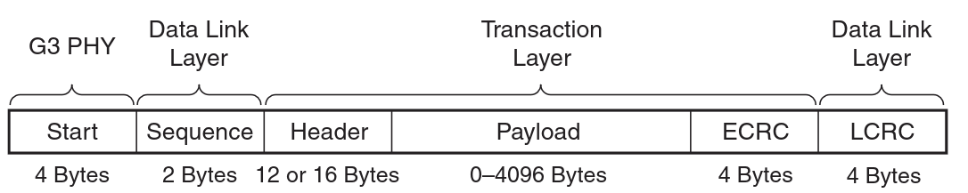
PCIe is a packetized protocol similar to the networking protocol. Which means there is a header overhead of communication, which varies across generations, as do the lane speed. The PCIe header can also be populated with some useful hints as we will see later.
| PCIe Gen | Encoding Overhead | Raw Speed/lane (GT/s) | Effective Bandwidth/lane | x8 (lanes) One-Directional Bandwidth |
|---|---|---|---|---|
| PCIe 1.0 | 20% | 2.5 GT/s | ~250 MB/s | ~2.0 GB/s |
| PCIe 2.0 | 20% | 5.0 GT/s | ~500 MB/s | ~4.0 GB/s |
| PCIe 3.0 | ~1.54% | 8.0 GT/s | ~985 MB/s | ~7.88 GB/s |
| PCIe 4.0 | ~1.54% | 16.0 GT/s | ~1.97 GB/s | ~15.75 GB/s |
| PCIe 5.0 | ~1.54% | 32.0 GT/s | ~3.94 GB/s | ~31.51 GB/s |
Numbers reflect theoretical payload throughput after encoding overhead, real-world payload is lower due to protocol overhead and flow control.
sample Transaction Layer Packet/ TLP
MMIO (Memory Mapped I/O)
Most high performance I/O devices are connected via PCIe. These devices have internal registers and memory. For example, a NIC has buffers to hold address of where to copy the incoming packets. To interact with these device’s registers/memory the CPU uses MMIO.
With MMIO, CPU doesn’t use specialized I/O instructions, instead the same physical address space is used to address both main memory 1 and the registers/memory of I/O devices. x86 primarily uses this method. 2 The address space is divided into chunks: some map to main memory, others to PCIe devices.
So how is this mapping created? During boot, the system queries the PCIe device’s Base Address Registers (BARs) to determine how much address space they need, and then reserves a chunk of the physical address space for them.
On Linux, you can see this mapping via sudo cat /proc/iomem.
The MMIO Access Flow
MMIO regions are typically marked as Uncacheable (UC) in the page tables. This is critical: if MMIO were cacheable, a CPU might read a “stale” register value from its own L1 cache instead of seeing a real changed value on the actual hardware.3
Snoop Filter (SF) acts as a socket-level directory, keeping track of all cachelines that are present in that socket caches. The exact information stored differs across architectures, skylake and later architectures use non-inclusive type L3 cache, in these cases snoop filter only tracks which cachelines are present in which core’s L1/L2 caches.
Caching & Home Agent (CHA) is responsible for serving core’s cacheline request after it misses L1/L2 core caches. In modern x86 architectures, post skylake the L3 is divided into slices and each slice handles a portion of addressable space 4. Each slice has its own CHA and SF. CHA looks into its L3 slice and its snoop filter to decide where the cacheline resides and handles coherencing and the transfer of cachelines.
When a CPU core accesses a virtual address:
The virtual address to physical address lookup happens. Along with the physical address we also get the memory type (Cacheable, Uncacheable, Write Combining)
a) If the memory is cacheable, the cores L1, L2 are searched. The result is served if its a cache-hit. Else the request goes to the L3/CHA slice corresponding to the address.
b) If the address is not cacheable, an MMIO controller determines if the physical address is MMIO or main memory
a) If the address corresponds to normal main memory and is cacheable, the CHA checks the L3 slice and snoop filter (to see if any other core has the cacheline). If yes, it snoops and serves the data. if no, it requests the IMC to fetch the data from main memory
b) If the address corresponds to normal main memory but uncacheable 5, requests IMC to fetch the address from main memory.
c) If address is MMIO, the request is by communicating with PCIe root complex
This flow is somewhat simplified and considers a single NUMA node/socket machine. In multiple NUMA nodes there are few more steps in case of cacheable memory to check if any other socket has the cacheline. Similarly to check if the MMIO address corresponds to the PCIe device connected on this socket or a remote socket and steer the request accordingly.
| |
NICs can also have registers/memory which are write-only. Some of these serve as doorbell, “set to true if packet is available in main memory buffer for NIC to DMA and send” which the NIC monitors. This memory may be marked as Write Combining instead of Uncacheable to benefit from write combining buffers.
DMA (Direct Memory Access)
Although with MMIO we can copy data to and from main memory to I/O devices using normal mov instructions (also referred as Programmed I/O , PIO), every MMIO read requires the CPU to wait for a round trip across the PCIe bus to get the data. MMIO writes dont have this problem, but still writing huge chunks of data by CPU to MMIO memory is very bad for throughput and wastes precious CPU time. To solve this, we have DMA.
DMA allows I/O devices to read from or write directly to main memory without constant CPU involvement. The CPU simply sets up a buffer, tells the device where it is using PIO, and then goes back to other work, while device DMA reads/writes the memory. In x86, DMA regions are cache-coherent. This means the hardware ensures that subsequent CPU accesses observe the device-written data correctly.
In case the data being DMA written is not a multiple of cacheline size or crosses a cacheline boundary then we enter the messy, time-taking case where the hardware has to combine the updated portion of cacheline with old values, sometimes called Read-modify-write/RMW cycle, which is why high-performance NICs try to align buffers and descriptors to cacheline boundaries to reduce these RMW DMA penalties.
IOMMU (I/O Memory Management Unit)
Similar to how the CPU doesn’t directly interact with physical addresses 6, I/O devices on modern machines also generally do not address main memory directly. Modern systems place an IOMMU between devices and physical memory, allowing device I/O virtual addresses to be translated before reaching CPU.
So If a piece of code wants to interact with a I/O device, say NIC then you request the kernel to create a virtual address, mapping to the MMIO of the device register C->B (in below diagram). You then allocate a buffer in RAM to be used for communication X->Y and then ask the kernel to create the IOMMU mapping Z->Y for the device to be able to access this memory. You pass this Z value to the device by writing into some defined register/memory by writing the value via C virtual address.
| |
Intel DDIO (Data Direct I/O)
In older systems the primary source and destination for DMA written I/O data was main memory.
So say CPU wants to send a packet to NIC:
CPU writes data to a chunk of memory.
This chunk of memory might not be in cache. The act of writing the data brings the chunk of memory into cache.
The CPU writes to some specific NIC’s register via MMIO, acting as a doorbell, to send the packet at that specific address on wire.
NIC triggers a DMA read. The read request reaches the PCIe complex and CHA.
a) If the data is present in cache its forwarded from there. In older xeon machines the cacheline was also evicted from the cache.
b) Else the data is accessed from main memory.
Similarly if NIC needs to write a packet to memory, the data is written into RAM, if the destination memory happens to be in CPU cache, its invalidated.
This was done in older systems because cache was considered a scarce resource.
Intel DDIO introduced in 2012, makes the LLC (Last Level Cache) the primary target for DMA reads and writes. DMA reads dont evict the cacheline. DMA writes, writes into LLC. If the destination memory location is present in LLC its updated and any copies in core’s private caches are invalidated. If the destination memory address doesn’t exist in LLC then its allocated and any core private copies invalidated.
The percentage of memory DDIO can use in LLC is capped. Typically only a subset of LLC ways can be used for DDIO allocation. Recall that caches are split into ways of associativity. A particular cacheline could be present in any one of the x-ways of associativity. DDIO is restricted to a subset of the ways of associativity. This means if the cacheline is present in one of the ways of associativity then its updated (and private core copies, if any invalidated), otherwise allocation of the cacheline only happens in one of the limited subset of the ways of associativity. The CPU uses all the ways of associativity for its reads and writes as usual.
Intel DDIO is transparent to the drivers and users. As in it works out of the box and doesn’t require any action to be used. It might be possible to tweak the limits on the subset of LLC used by DDIO. 7
How it works:
- DMA Reads: Data is fetched from cache if present, without evicting it. If not present its fetched from main memory
- DMA Writes: Data is written directly into LLC. If the cacheline isn’t there, it’s allocated in a limited “window” (a subset of cache ways) to prevent a flood of I/O data from evicting the CPU’s working set.
If the NIC is attached to a different NUMA node than the CPU core processing the packets then the cacheline may repeatedly bounce between the nodes over interconnect 8 incresing latencies. So its better to the pin the accessing core on the same node the PCIe device is directly connected to.
PCIe TPH and Steering Tags
TPH (TLP/Transaction Layer Packets Processing Hints) is a PCIe feature that allows devices to attach metadata to transactions. PCIe packets can have TPH info populated in its headers. One of the possible hints that can be placed in TPH are steering Tags (ST). There are special values that can hint the CPU’s memory subsystem on where to place the data (e.g. which core’s L2 to preferably place the data in). Obviously, The NIC needs to have support for TPH and the architecture should have support for steering tags, and the granularity of hints depend on the platform and architecture.
SMART DATA CACHE INJECTION (AMD SDCI)
AMD EPYC Zen 5, has support for steering tags that allow a device to hint that data should be preferably placed into a core’s L2 cache, AMD calls this SDCI . This bypasses the L3 entirely for the most latency-sensitive data, placing the packet exactly where the processing thread is running.
Some Solarflare NICs have support for this 9.
NICs
Along with standard NICs and their drivers, we also have “Accelerated” NICs (like exanic, or solarflare) with support these high 10Gbps/50Gbps network speeds along with:
- Kernel Bypass: Allows userspace packet processing without kernel involvement in the hot path
- Low Latency PIO: Direct CPU-to-NIC writes for small packets.
- Hardware Offloads: Checksum offloading, TSO (TCP Segmentation Offload), and even onboard FPGA processing.
The Flow: Receive & Transmit
NIC Receive:
Packet arrives from wire.
NIC performs DMA write to a pre-allocated buffer.
a) If DDIO is active, data lands in L3/LLC.
b) if SDCI is active, data may be injected into L2.
Once the data has been written, the CPU needs to be notified. In Kernel Bypass scenarios, the CPU often polls a memory location. In standard networking, the NIC raises an Interrupt.
| |
NIC Transmit:
- Method 1 (DMA): CPU writes packet to a DMA region and updates a NIC register (which acts like a doorbell informing data is available). This can be as simple as updating a boolean or writing a index/memory location corresponding to the packet’s memory. The NIC then DMA-reads the data.
- Method 2 (PIO): For ultra-low latency and very small packets, it can be faster for CPU to write packet data directly into a special memory region on the NIC 10 itself using PIO. This skips the NIC’s DMA read trip over PCIe, and can result in lower latency for small packets. This special memory region can benefit from being marked as Write Combining to utilize write combining buffers.
| |
In the next articles in this series, we will go over the software side of how received packets are written, Ring Buffers, Descriptors, Hugepages and some of the accelerated NICs workings.
Further Reading
- Understanding performance of PCIe
- Linux DMA and MMIO
- Intel DDIO
- Using TPH and ST
- AMD Smart Data Cache Injection
Memory that resides in RAM ↩︎
x86 still support traditional
INOUTinstructions but mainly use MMIO for modern devices ↩︎Write Combining also generally doesn’t work as it permits speculative reads ↩︎
A hash of the physcial address decides which slice handles it ↩︎
Some physical memory regions may intentionally be mapped as uncacheable, in which case accesses bypass CPU caches and go directly to RAM ↩︎
at least when running in userspace ↩︎
controllable by MSRs in some machines ↩︎
UPI: UltraPath Interconnect is the name of the low-latency interconnect between sockets in skylake and beyond. AMDs equivalent is called “Infinity Fabric” ↩︎
Expected that new AMD EYPC features are supported by new AMD Solarflares ↩︎
provided NIC has this functionality ↩︎